- [email protected]
- (+1) 5103455000
Special PCB
- Ceramic PCB
- Copper Coin PCB
- Gold Plating PCB
- Heavy Copper PCB
- Thick Copper PCB
- Transparent Glass PCB
- View All PCB Products
FPC & Rigid-flex
- Rigid Flex PCB
- Single Layer Flex PCB
- Multilayer Flex PCB
Standard PCB
- Rohs Complaint PCB Manufacture
- Tg180/High Tg PCB
- 6 Layer Blue Solder Mask PCB
- Heat Sink PCB
- LED PCB from China
Metal Base PCB
- Copper Base PCB
- Aluminum PCB
- METAL CLAD PCB
- Super Pillar MC PCB
- IMS PCB/Insulated metal substrate PCB
- 2L/ Double Sided Alu PCB
PCB Assembly
- PCBA (PCB+ Components+ Assembly)
- Light / LED PCB Assembly
- Fast Turnaround PCBA
- Turnkey PCB Assembly
- VIRTUAL FACTORY TOUR
- Manufacturing Equipment
- Certification And IPC Standard

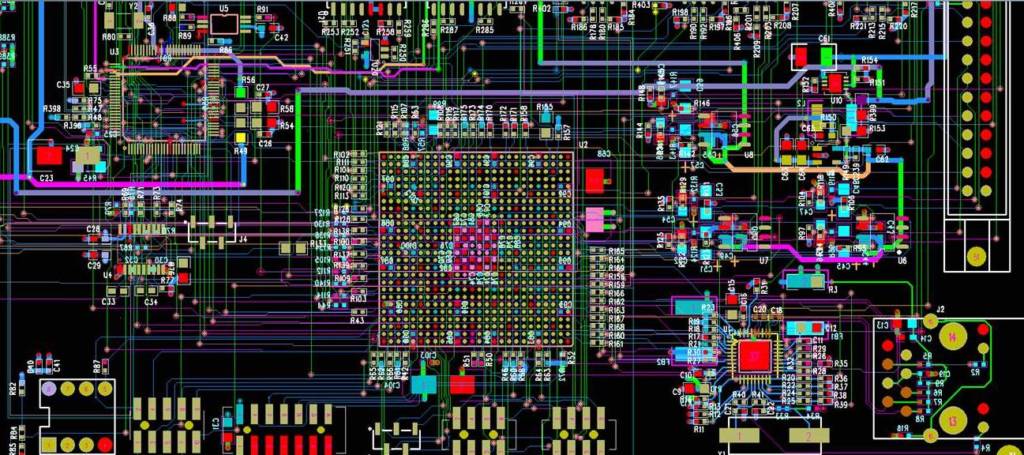
Comprehensive Guide to PCB Layout Design: Tips, Basics, and Guidelines
Printed Circuit Boards (PCBs) are the backbone of modern electronic devices, acting as a platform for connecting and supporting various electronic components. An efficient and well-structured PCB layout is crucial for ensuring optimal performance, signal integrity, and reliability of electronic devices. In this comprehensive guide, we will explore the essential aspects of PCB layout design, from the basics to advanced guidelines and helpful tips.
Table of Contents
Our recommended led light pcb.

Light PCB assembly is the process of assembling and soldering electronic components onto a printed circuit board (PCB) to form a functional electronic device. The PCB material should be chosen based on factors like fire retardant, dielectric constant, loss factor, tensile stability, glass transition temperature, and Z-axis expansion coefficient. Common materials used for Light PCBs are CEM-1, CEM-3, FR-4, aluminum, and copper alloys. The material should be selected based on the specific requirements of the electronic device being produced.
Shenzhen PCB assembly manufacturer is the ideal place for your Light PCB assembly needs. We can assist you in assembling everything from industrial high-power LEDs to commercial flood LEDs.
Understanding PCB Layout Design:
PCB layout design is the process of arranging electronic components, conductive traces, power planes, and other elements on a circuit board to facilitate the flow of electrical signals and meet the functional requirements of the electronic system. The layout design is a critical step in the PCB design process, as it directly impacts the electrical performance, electromagnetic interference, thermal management, and manufacturability of the final product.
How to Design a PCB Layout
Designing a PCB (Printed Circuit Board) layout can seem intimidating at first, but with the right tools and understanding of the process, it becomes more manageable. Here’s a general guide to help you design a PCB layout:
Schematic Design: Start by creating a schematic diagram of your circuit. This will help you plan the connections between components and understand the overall layout of your PCB.
Choose PCB Design Software: Select a PCB design software that suits your needs and level of expertise. Some popular options include Altium Designer, Eagle, KiCad, and OrCAD. These tools offer various features for schematic capture, PCB layout, and design verification.
Component Placement: Import the components from your schematic into the PCB design software. Arrange them on the board to optimize signal flow, reduce trace lengths, and ensure proper clearances between components.
Routing Traces: Connect the components using traces (copper lines) on the PCB. Consider the current-carrying capacity, signal integrity, and noise immunity when routing traces. Keep traces short and direct to minimize signal interference.
Power and Ground Planes: For better noise reduction and improved power distribution, allocate separate power and ground planes. Connect all ground points to the ground plane to create a low impedance return path for current.
Signal Integrity: Check for signal integrity issues such as reflections and crosstalk. Use controlled impedance traces for high-speed signals to maintain signal integrity.
Design Rules Check (DRC): Perform a design rules check to ensure that your layout complies with the fabrication capabilities of your PCB manufacturer. The DRC will catch errors like trace width violations, clearance violations, and other manufacturing-related issues.
Thermal Considerations: If your circuit generates significant heat, design the PCB layout with proper heat dissipation in mind. Use thermal vias and heatsinks as necessary.
Silkscreen and Documentation: Add component designators, reference labels, and any other important information to the silkscreen layer for easy assembly and debugging.
Design Verification: Before sending your design for manufacturing, perform thorough design verification. Use tools within your PCB software to check for errors and simulate the circuit’s performance if needed.
Gerber Files Generation: Generate the Gerber files, which are the standard format used by PCB manufacturers to fabricate the PCB.
Manufacturing: Choose a reputable PCB manufacturer and submit your Gerber files along with any other required documentation. Review the manufacturer’s guidelines and requirements to ensure a successful fabrication process.
Assembly: Once you receive the fabricated PCBs, you can assemble the components yourself or use a PCB assembly service.
PCB Layout Basics:
Before delving into advanced concepts, let’s cover the fundamental components of a PCB layout:
PCBs are often designed with multiple layers to accommodate complex circuitry. Common layers include top and bottom copper layers, power and ground planes, and signal layers. Each layer serves a specific purpose in the overall functionality of the PCB.
b. Components:
Electronic components, such as resistors, capacitors, integrated circuits (ICs), and connectors, are placed strategically on the PCB to ensure efficient signal flow and minimize signal distortion. Proper component placement also helps in thermal dissipation and ease of assembly.
c. Traces and Vias:
Traces are conductive pathways that connect various components on the PCB. Vias are plated holes used to establish electrical connections between different layers of the PCB.
d. Power Planes:
Dedicated copper planes are used for distributing power and ground throughout the PCB. These planes help in noise reduction and provide a stable power supply to the components.
PCB Layout Design Process:
The PCB layout design process typically involves the following steps:
a. Schematic Design:
The circuit schematic is the initial representation of the circuit’s electrical connections and components. It serves as a blueprint for the subsequent PCB layout design.
b. Component Placement:
During this stage, designers strategically place the components on the PCB to optimize signal flow, minimize trace length, and ensure efficient thermal management.
c. Routing:
The routing process involves creating conductive pathways (traces) between components to establish electrical connections. Proper routing techniques are essential to avoid signal interference and crosstalk.
d. Design Rule Check (DRC):
After completing the layout, designers perform a DRC using PCB design software. The DRC verifies that the layout complies with manufacturing and design rules, such as trace width, spacing, and clearance requirements.
e. Gerber Generation:
Once the layout is verified, designers generate Gerber files, which are industry-standard files used by PCB manufacturers to fabricate the board.

PCB Layout Tips:
Designing an efficient PCB layout requires attention to detail and adherence to best practices. Here are some valuable tips for creating a successful PCB layout:
a. Component Placement Optimization:
Group related components together and place high-speed components closer to each other and the power source to minimize signal delays and noise.
b. Signal Traces and Routing:
Pay attention to trace width and impedance control for signal integrity. Separate high-speed and low-speed signal traces to reduce interference.
c. Thermal Considerations:
Optimize thermal dissipation by placing components with high heat dissipation needs close to thermal vias or heat sinks.
d. Ground Plane Design:
Utilize dedicated ground planes to improve noise immunity and reduce ground loops.
e. Design Rule Checks (DRCs):
Regularly perform DRCs to identify and rectify layout errors, ensuring compliance with design specifications.
f. Manufacturer Collaboration:
Engage with the PCB fabrication house early in the design process to understand their capabilities and avoid potential manufacturing issues [2].
PCB Layout Guidelines:
To ensure a successful PCB layout, follow these essential guidelines:
a. Component Orientation:
Keep component orientations consistent to facilitate ease of assembly.
b. Trace Width and Spacing:
Use appropriate trace widths and spacing to handle current-carrying capacity and impedance control.
c. Power Plane Design:
Implement proper power plane structures for distributing power efficiently and minimizing voltage drops.
d. Signal Integrity and High-Speed Design:
Employ signal integrity techniques for high-speed signal routing to prevent signal degradation and reflections.
e. Silkscreen and Assembly Markings:
Provide clear silkscreen markings and assembly indicators for proper component placement during assembly.
Pcb layout software
Altium Designer: Altium Designer is a widely-used PCB design software known for its intuitive user interface, powerful features, and extensive component libraries. It offers tools for schematic capture, PCB layout, 3D visualization, signal integrity analysis, and manufacturing file generation.
Cadence Allegro PCB Designer: Cadence Allegro is a professional-grade PCB design tool commonly used in the industry. It provides advanced features for high-speed PCB design, differential pair routing, constraint-driven layout, and collaboration between team members.
Eagle PCB: Eagle PCB is a user-friendly PCB design software suitable for hobbyists and small projects. It offers a free version for limited designs and a paid version with extended features, such as multilayer board support and larger board sizes.
KiCad: KiCad is an open-source PCB design software that has gained popularity among hobbyists and small businesses. It provides a suite of tools for schematic capture, PCB layout, 3D visualization, and extensive community support.
OrCAD PCB Designer: OrCAD PCB Designer, developed by Cadence, is a comprehensive PCB layout tool with features like constraint-driven routing, powerful signal and power integrity analysis, and seamless integration with other tools in the OrCAD suite.
PADS (Mentor Graphics): PADS is a powerful PCB design software tailored for medium to large-scale design projects. It offers a scalable platform with various levels of functionality, making it suitable for both beginners and advanced PCB designers.
Proteus PCB Design: Proteus PCB Design is a user-friendly software that combines schematic capture, simulation, and PCB layout in a single package. It is often favored by hobbyists and students for its ease of use.
DipTrace: DipTrace is a versatile PCB design tool suitable for projects of different sizes. It offers an intuitive interface, 3D modeling, a vast component library, and extensive manufacturing file support.
EasyEDA: EasyEDA is an online PCB design tool that allows users to design and share PCB layouts directly in a web browser. It offers schematic capture, PCB layout, and cloud-based collaboration features.
DesignSpark PCB: DesignSpark PCB is a free, entry-level PCB design software developed by RS Components. It provides a user-friendly interface and basic PCB design capabilities.
Conclusion:
A well-designed PCB layout is integral to the success of any electronic device. Understanding the basics, following best practices, and incorporating design guidelines are essential for creating efficient, reliable, and manufacturable circuit board layouts. By combining technical expertise, attention to detail, and collaboration with experienced PCB manufacturers, designers can develop cutting-edge electronic products that meet the demands of today’s technology-driven world. Remember, continuous learning and staying updated with the latest advancements in PCB design tools and techniques will further enhance the quality of PCB layouts and contribute to the development of innovative electronic products.

I am Peter Gong. I have been working in PCB and PCBA industry for 15+ years now. I have been a part of the PCB revolution with my dedication to circuit board technologies and creative ideas. I write in FX PCB to impart my knowledge on PCB and PCBA for all circuit board lovers, manufacturers, and users.
Our Recommended Products for You

Ceramic PCB AIO203 Material 3

Ceramic PCB 16

Aluminum Nitride PCB Manufacturer in China

Ceramic PCB 14

Ceramic PCB 13

Ceramic PCB 12

Product & Services
- CERAMIC PCB
- FPC & RIGID FLEX PCB
- Privacy Policy
Payment Methods
- Bank Transfer
Shippment Options
Submit Your Enquiry
WhatsApp us
Top Tips for Successful PCB Layout Design: Guidelines and Best Practices
Printed circuit board (PCB) layout is a crucial step in the design and development of electronic circuits. A well-designed PCB layout can ensure the optimal performance and functionality of an electronic device. PCB layout involves the placement of components on a board and routing of electrical connections between them. Designers must consider various factors such as signal integrity, thermal management, and electromagnetic interference (EMI) when creating a PCB layout.
In this article, we will provide an overview of PCB layout design, including guidelines and best practices. We will also discuss the importance of PCB layout design and its impact on the overall performance of electronic devices. Additionally, we will explore the use of free PCB layout software, the steps involved in creating a PCB layout, and the benefits of outsourcing PCB layout services.
By following PCB layout guidelines and best practices, designers can ensure that their PCB layouts are optimized for performance, reliability, and manufacturability.
PCB Layout Guidelines
PCB layout guidelines are a set of rules and best practices that designers follow to ensure that their PCB layouts are optimized for performance, reliability, and manufacturability. PCB layout guidelines help designers avoid common mistakes and ensure that their PCB layouts meet the desired specifications. In this section, we will discuss some of the most important PCB layout guidelines.
Component Placement
Component placement is one of the most critical aspects of PCB layout design . Placing components in the right locations can help reduce noise, improve signal integrity, and optimize thermal management. Some guidelines to follow for component placement include:
Place components based on their function and importance
Group related components together
Place high-speed components close to each other
Place heat-generating components away from sensitive components
Place components on one side of the board to reduce manufacturing costs
Trace Routing
Trace routing involves the routing of electrical connections between components on the PCB. Proper trace routing is essential for ensuring signal integrity, reducing noise, and optimizing thermal management. Some guidelines to follow for trace routing include:
Use short, direct traces whenever possible
Keep traces as wide as possible to reduce resistance and heat
Place ground and power planes close to high-speed traces
Use differential pairs for high-speed signals
Avoid crossing traces to reduce noise
Signal Integrity
Signal integrity is a critical consideration in PCB layout design. Poor signal integrity can result in signal distortion, signal loss, and electromagnetic interference (EMI). Some guidelines to follow for signal integrity include:
Use controlled impedance traces for high-speed signals
Minimize the length of high-speed traces
Use decoupling capacitors to filter noise
Thermal Management
Thermal management is essential for ensuring the reliability and longevity of electronic devices. Poor thermal management can lead to overheating and premature failure of components. Some guidelines to follow for thermal management include:
Use copper pours to dissipate heat
Use heat sinks or thermal vias to improve heat dissipation
Avoid placing components in areas with poor airflow
Ensure that the PCB layout allows for adequate space for cooling components
Best Practices for PCB Layout Design
PCB layout design is a complex process that requires careful consideration of various factors. Following best practices can help designers optimize their design process and create high-quality PCB layouts. In this section, we will discuss some of the best practices for PCB layout design.
Tips for Optimizing the Design Process
Optimizing the design process is crucial for PCB designers to save time, reduce errors, and improve the overall quality of the PCB layout. Here are some tips for optimizing the design process:
Start with a Clear Design Objective and Specifications:
The first step in optimizing the design process is to have a clear design objective and specifications. The designer should have a thorough understanding of the project requirements and constraints, and should develop a design plan that meets these requirements.
Use a Consistent Design Methodology:
Using a consistent design methodology can help to improve the efficiency of the design process. The designer should use a standardized approach to component selection, schematic capture, and PCB layout. This helps to reduce errors and ensure that the design process is streamlined.
Use Design Review and Verification Tools to Catch Errors Early:
Design review and verification tools can help to catch errors early in the design process, reducing the risk of costly errors later on. These tools can include schematic capture and PCB layout software , as well as third-party simulation and analysis tools.
Use Modular Design to Simplify the Layout Process:
Modular design involves breaking the design down into smaller, more manageable modules. This can help to simplify the layout process and reduce errors. It also allows designers to reuse modules in future designs, saving time and effort.
Use a Standardized Naming Convention for Components and Nets:
Using a standardized naming convention for components and nets can help to reduce errors and improve the efficiency of the design process. A standardized naming convention can also help to make the design more easily readable and understandable for other members of the design team.
Importance of Component Placement and Trace Routing
Component placement and trace routing are critical aspects of PCB layout design. Proper component placement and trace routing can help reduce noise, improve signal integrity, and optimize thermal management. Some best practices for component placement and trace routing include:
● Place components based on their function and importance
● Use short, direct traces whenever possible
● Keep traces as wide as possible to reduce resistance and heat
● Use ground and power planes to reduce noise and improve signal integrity
● Use differential pairs for high-speed signals
Considerations for Signal Integrity and EMI/EMC
Signal integrity and electromagnetic interference (EMI) and electromagnetic compatibility (EMC) are critical considerations in PCB layout design. Poor signal integrity and EMI/EMC can result in signal distortion, signal loss, and interference with other electronic devices. Some best practices for signal integrity and EMI/EMC include:
● Use controlled impedance traces for high-speed signals
● Minimize the length of high-speed traces
● Use decoupling capacitors to filter noise
● Use shielding to reduce EMI/EMC
● Follow EMI/EMC regulations and guidelines
Best Free PCB Layout Software
Free PCB layout software can be an effective tool for designers, especially those with limited budgets. Free PCB layout software provides designers with the ability to create high-quality PCB layouts without the need for expensive software. Some popular free PCB layout software options include:
DesignSpark PCB
How to Create a PCB Layout
Creating a PCB layout is a complex process that requires careful planning and execution. In this section, we will discuss the steps involved in creating a PCB layout.
Design Planning
The first step in creating a PCB layout is to plan the design. This involves defining the requirements, selecting components, and creating a schematic diagram. The schematic diagram is used to map out the electrical connections between components and serves as a blueprint for the PCB layout.
Once the schematic diagram is complete, the next step is to place the components on the PCB layout. The placement of components is critical for optimizing signal integrity, reducing noise, and optimizing thermal management. Some best practices for component placement include:
After placing the components, the next step is to route the traces that connect them. Proper trace routing is critical for ensuring signal integrity, reducing noise, and optimizing thermal management. Some best practices for trace routing include:
Use ground and power planes to reduce noise and improve signal integrity
Testing and Verification
After completing the PCB layout, the next step is to test and verify its functionality. This involves performing electrical tests, such as continuity and resistance checks, and verifying that the PCB layout meets the design specifications.
Manufacturing
Once the PCB layout is tested and verified, the final step is to manufacture the PCB. This involves transferring the design to a physical PCB and soldering the components to the board.
Creating a PCB layout is a complex process that involves careful planning, component placement, trace routing, testing, and verification. By following best practices, designers can create high-quality PCB layouts that meet the desired specifications. Proper component placement and trace routing, testing and verification, and working with a reputable PCB manufacturer can help ensure that the PCB layout is optimized for performance, reliability, and manufacturability.
PCB Layout Services
What are pcb layout services.
PCB layout services involve creating a physical layout of a printed circuit board (PCB) based on a schematic diagram. PCB layout services can be provided by a variety of companies, ranging from small design firms to large contract manufacturers.
PCB layout services typically include the following:
Component placement
Trace routing
Testing and verification
Design rule check (DRC)
Manufacturing support
Why are PCB Layout Services Important?
PCB layout services are important for several reasons. First, the layout of a PCB is critical for optimizing signal integrity and reducing noise. A well-designed PCB layout can ensure that the device functions correctly and meets the desired specifications.
Second, PCB layout services can save time and money in the electronic design process. By outsourcing PCB layout services, designers can focus on other aspects of the design process, such as component selection and testing. This can help speed up the design process and reduce costs.
Finally, PCB layout services can help ensure that the PCB layout is optimized for manufacturability. A well-designed PCB layout can help reduce manufacturing costs and improve yield.
Choosing a PCB Layout Service Provider
Choosing a PCB layout service provider can be a daunting task. There are many factors to consider, including experience, expertise, and cost. Here are some tips for choosing a PCB layout service provider:
● Look for a company with experience in your industry or application.
● Check the company's credentials and certifications.
● Ask for references and check them.
● Consider the company's design process and tools.
● Compare pricing and services.
In conclusion, PCB layout design is a critical aspect of electronic design that requires careful planning and execution. By following guidelines and best practices, designers can create high-quality PCB layouts that meet the desired specifications, optimize signal integrity, and reduce noise.
Some of the key guidelines and best practices for PCB layout design include proper component placement, trace routing, and testing and verification. Designers should also consider factors such as thermal management, EMI, and manufacturability when creating a PCB layout.
Overall, by following best practices and working with a reputable service provider, designers can create PCB layouts that meet the desired specifications and perform reliably in the field.
Related Articles:
PCB Basics : Design Guidelines
Recent Posts
• Unlocking the Potential of Via Design in PCBs: Enhancing Performance and Connectivity
Mar 14, 2024
• PCB Basics: Differential Pair in PCB design
Mar 13, 2024
• PCB Basics: 50ohm PCB Trace with simple PI matching
• The Critical Role of PCB Trace Width and How to Calculate It
Mar 6, 2024
• Basic Design of Solder Mask
Feb 28, 2024
- Certifications
- We’re Hiring
- Call 1-800-444-6817
- Share on LinkedIn
- Share on Twitter
- Share on Facebook
Your Guide to PCB Design Basics & Steps

Your time is valuable, which is why you want to design your printed circuit board correctly from the start. In our comprehensive guide, we cover everything you need to know, including PCB design basics and steps, materials and composition, best practices, and more so that you’re prepared to design the best possible printed circuit board.
PCB Design Basics
Step by Step PCB Design Guide
PCB Design Best Practices
Pcb composition & materials, pcb layout capabilities, pcb and flex design basics.
A printed circuit board (PCB) is a flat plate or base of insulating materials that contains a pattern of conducting material and components, and some projects can be quite complex. But all PCBs have to start somewhere — and that’s with design.
Why are PCB design basics so important? Multiple extensive revisions can seriously delay the completion of your project — costing you time and money. It’s important to work with engineering experts from the beginning so that you can design for manufacturability and ensure a final, cost-effective product that works efficiently and effectively.
Step-by-Step PCB Design Guide
From the initial drawings to the final files, here are the 9 steps toward designing a printed circuit board:
1. Understand the electrical parameters.
Before starting a PCB design, you should know and understand the electrical parameters of the system, including:
- Current maximums
- Signal types
- Capacitance limitations
- Impedance characteristics
- Shielding considerations
- Type and location of circuit components and connectors
- Detailed net wire listing and schematic
2. Creating the schematic.
One of the first steps is always creating a schematic, which refers to the design at the electrical level of the board’s purpose and function. At this point, it’s not yet a mechanical representation.
3. Use a schematic capture tool to create your PCB layout.
The right PCB provider will work with principal engineers to develop a schematic with a software platform such as Mentor PADS® , Allegro , or Altium , which shows you exactly how your board will operate and where the components will be placed. After you create your schematic, the mechanical engineer will load the design and determine how it will fit in the intended device.
4. Design your PCB stackup.
This is important to consider early on in the PCB design stage due to impedance, which refers to how much and how quickly electricity can travel down a trace. The stackup plays a role in how the mechanical engineer can design and fit the PCB into the device.
5. Define design rules and requirements.
This step is largely dictated by standards and acceptability criteria from the IPC , which is the industry association for PCB and electronics manufacturing. These standards tell you everything you need to know regarding PCB manufacturing. An important tip: Find a PCB layout provider who is extremely familiar with IPC standards; this can help you avoid major revisions and project delays.
6. Place your components.
In many cases, the customer and PCB provider will discuss design and layout guidelines when it comes to the placement of components. For example, there may be standards indicating that certain components cannot be placed near others because they create electrical noise in the circuit. The PCB provider will have data sheets on every component (in most cases these are connectors), which will then be placed in the mechanical layout and sent to the customer for approval.
7. Insert drill holes.
This step is driven by the components and a connection. About half of the flex circuits on the market are double-sided, which means they have connection to the drill hole on the bottom layer.
8. Route the traces.
After you’ve placed the components and drill holes, you’re ready to route the traces, which means connecting segments of the path.
9. Add labels and identifiers.
Now is the time to add any labels, identifiers, markings, or reference designators to the layout. Reference designators are helpful in showing where specific components will go on the board.
10. Generate design/layout files.
This is the final step in the layout process. These files contain all the information pertaining to your printed circuit board, and once they have been generated, your PCB is now ready for fabrication and manufacturing and assembly .
It’s important to communicate with the PCB or flex application engineer during the beginning of any PCB design job and discuss everything you need or require for your project. Open and constant communication with your PCB provider ensures that you’re both on the same page, which can reduce the need for multiple extensive revisions.
While it is rare that a printed circuit board is 100% perfectly designed on the first try, communication will help ensure that your PCB is properly designed from the start and that any revisions are not major ones that will derail your project and timeline.
When you submit a design, you also need to have the right board size, trace width, materials, component placement, and tolerances. Plus, in the case of flex, you’ll need to determine whether the design is static, partly flexible, or dynamic.
It’s also important to consider the environment in which the product has to function. Is the printed circuit board or flex circuit designed for a non-extreme environment, such as your cell phone, or the highest of extremes, such as an explosion?
You’ll likely have questions about the PCB design and layout process, which means it’s best to find a reputable PCB provider with extensive engineering experience who can answer your questions and ensure a smooth project from start to finish.
A copper-clad substrate or polyimide-based film is often used for flex circuits, and FR4 (or an FR4 stiffener) is used for rigid-flex. FR4 allows you to build up the layers as the technology content is created.
A solder mask is also used, which is a technique where everything on the circuit board is coated with an epoxy-based LPI or cover coat for flex, except the contacts to be soldered, the gold-plated terminals of any card-edge connectors, and fiducial marks.
PCBs also include a legend application, which are the decals and reference designators in epoxy ink on a board. The name refers to the method of application in which the ink is automatically applied similar to ink jet printers
Cirexx can configure digital, analog, mixed signal technology, controlled impedance, matched length pairs DDR, RF layout, and high speed signals up to 100+ GHz for all of the following PCB structures:
- Flex circuits
- Rigid-flex circuits
- Rigid circuits
- Hybrid circuits
- BGA/micro BGA
- Buried vias
- Surface mount/thru-hole/chip (die)
- High-Density Interconnect (HDI)
Are you looking for help with your next PCB design? Contact us today to learn more about our capabilities or to consult with one of our engineering experts on your next project.
Don Kaufman is our Business Development Manager and has been with Cirexx International since 2006. He has over 33 years of sales and technical experience in the printed circuit board industry, which provides intrinsic value to customers. Don has extensive knowledge regarding integrated circuits, materials, specialty laminates, chemicals and equipment. He also prides himself on staying current with the very latest techniques and procedures in PCB Layout and manufacturing.
10 Questions to Ask Before Choosing Your Next PCB Solutions Provider
From Certifications and Experience to Quality Assurance and Timelines: What You Need to Know Are you in the market for…

Related Articles

PCB Surface Finish Types: Choosing ENIG, HASL, or Others
A printed circuit board (PCB) surface finish has two main functions: To prevent the copper from oxidizing and to provide a solderable surface.
Your Guide to Flexible PCB Design & Layout
All printed circuit boards essentially perform similar functions, but there are three main types — rigid, rigid-flex, and flex — which all differ in terms of design and construction.

PCB Vias [Your Full Guide]
Vias are an essential part of the multi-layered printed circuit board (PCB) design and manufacturing process – but what are they exactly? And how do the various kinds differ from one another? In thi…
- PCB Design Guidelines For Better Layout
Here are some simple PCB design guidelines that can help you create better board layouts.
Board size and trace width
There are always limits to how big your board can be, how thin your traces can be and the smallest drill size you can use.
Start out by checking the capabilities of your PCB manufacturer . They usually put this information out on their web page. Sometimes they supply a Design Rule Check file that can be loaded right into your PCB design software .

First, resize your board so that it does not exceed the capabilities of the manufacturer you have chosen.
Next, choose a trace width. It must be at least the size of the smallest allowed trace width, but should generally be thicker because thin traces are more vulnerable to damage when soldering.
The more current that is going to flow through the trace, the thicker it should be. This is to make sure the trace does not heat up. If you have a lot of space on your circuit board, start with 20 mil trace width for signals and 30-40 mil for power traces.
Placement of components
Place your components in a similar way as in your schematics. This makes it easier to troubleshoot your circuit if needed later on.
Pay attention to connectors and large components. Connectors should be placed on the side for simple connection.

Make Your First Printed Circuit Board
Download my guide with all the steps you need to design your first printed circuit board (PCB) from scratch.
If you are going to place the finished PCB in a box, keep in mind any large components and how they will fit in the box when you are going to assemble your electronic project.
If your electronic circuit consists of any decoupling capacitors, make sure you place them close to the pins they are meant for.
Your components should all have labels with the name and part value printed on the board. This makes it easier to solder the circuit board and to troubleshoot it later on.
A useful rule-of-thumb is always to label connectors that are to be connected to the outside with descriptive names. Add names for each pin on a pin header.

PCB design guidelines for horizontal and vertical routing
If you are using a two-layer circuit board, one of the best PCB design guidelines to follow is to route one layer horizontally and the other vertically.
For more complex boards, the addition of a ground plane can simplify your routing effort.

Trace angles
If you are making an RF circuit board, you should avoid 90-degree angles on your PCB traces. Otherwise, weird effects might occur.
Also, 45-degree angles look more professional, so you should just get into the habit of making 45-degree angles from the start.

Visual check
When you have completed your board, you should always print your board on paper and check it for any problems with connectors and such.
Many times I have done the mistake of putting a pin header the wrong way or something else that could have been avoided if I had just taken the time to print my circuit on paper and check for those things.
Return from PCB Design Guidelines to PCB Design
More PCB Design Tutorials
- Introduction to PCB Design
- How To Create Your Own Printed Circuit Boards
- Printed Circuit Board Guide For Beginners
- Free PCB Design Software
- Cheap PCB Design Process
- PCB Design Rules
- PCB Manufacturing Preparation
- PCB Terminology 101
- The Gerber Format
- Using a Gerber Viewer To Check For Errors
- How To Build A Circuit In 6 Steps
- Develop Your Own Electronic Product
5 thoughts on “PCB Design Guidelines For Better Layout”
Just thank u For this.Really i am saying this from the bottom of my heart.
Glad I can help =)
it was really good to study will about pcb design
Hello Oyvind,
Do you have a practical example of the PCB design guidelines for horizontal and vertical routing? Had never heard this guideline so will like to learn more about it.
Hey Roberto,
This is just because if you route one signal on the top layer and one on the bottom layer from top to bottom in the middle of your board – you have no way of going from the left to right (or vice versa) with any other signals. By routing one direction with one layer, and the other direction with the other layer – you make sure you don’t block the way for more signals to be routed.
Best, Oyvind
Leave a Comment Cancel reply
- Knowledge Center /
Top PCB Design Guidelines
It’s easy to leave the PCB design guidelines as an afterthought, spending most of your time focusing on circuit design, functionality, and component selection. However, not providing attention to PCB layout basics can lead to a design that translates poorly from the digital domain to physical reality. Thereby making it more difficult to fabricate.
The top 5 PCB design guidelines we can suggest to improve manufacturability, functionality, and reliability are discussed below.
1. Fine-Tune Component Placement
The component placement requires strategic consideration of the available PCB real estate available on your board. This process can be challenging. However, placement of electronic components will determine how easy the board is to manufacture, as well as how well it meets your design requirements.
There are many PCB layout rules to consider during component placement. While general board layout guidelines tell you to place components in order of connectors, power circuits, precision circuits, critical circuits, etc, there are also several specific board layout guidelines to consider.
Orientation: Be sure to orient similar components in the same direction as this will help with effective routing in PCB design . It also helps ensure an efficient and error-free soldering process during assembly.
Placement: Avoid placing components on the solder side of a board that would rest behind plated through-hole components.
Organization: It’s recommended to place all your surface mount devices (SMD) components on the same side of your board according to SMD PCB design rules. All through-hole (TH) components should be placed on the top side of your board to minimize the number of assembly steps.
When using mixed-technology components (through-hole and surface mount components), manufacturers might require an extra process to assemble your board, which will add to your overall printed circuit board costs.
2. Power, Ground & Signal Traces
After component placement, route your power, ground, and signal traces to ensure your signals have a clean and trouble-free path of travel. Here are some guidelines to keep in mind for this stage of your layout process:
Place your power and ground planes internal to your printed circuit board keeping them symmetrical and centered. This will help to prevent your board from bending, which will also affect whether your components are properly positioned. Note that this is not possible on a two-layer board as you will not have any room for components. To power your ICs, it’s recommended to use common rails for each supply, ensure you have solid and wide traces, and also avoid daisy-chaining power lines from part to part.
Next connect the signal traces to match your schematic guidelines. PCB layout best practices recommend that you always keep traces as shortand directas possible between components. If your component placement forces horizontal trace routing on one side of the board, then always route traces vertically on the opposite side.
Printed circuit board design rules and PCB layout guidelines become more complex as the number of layers in your stack-up increases. Your routing strategy will require alternating horizontal and vertical traces in alternating layers unless you separate each signal layer with a reference plane.
Your printed circuit board design will likely require different nets that will carry a wide range of currents, which will dictate the required net width. It’s recommended to provide a 0.010” width for low current analog and digital signals. Printed circuit board traces that carry more than 0.3 A should be wider.
3. Keep Things Separate
Large voltage in power circuits and current spikes can interfere with low voltage and current control circuits. To minimize this interference issue, it’s recommended to:
Separate power ground and control ground for each power supply stage. If you do have to tie them together in your PCBs, make sure it’s toward the end of your supply path.
If you have placed your ground plane in the middle layer be sure to place a small impedance path to reduce the risk of any power circuit interference and to help protect your control signals. The same guideline can be followed to keep your digital and analog ground separate.
To reduce capacitive coupling due to the placement of a large ground plane and the lines routed above and under it, try to have your analog ground crossed only by analog lines.
4. Minimize Heating Issues
Heat dissipation can degrade performance. Some guidelines to minimize include:
Identify Problem Parts -considerwhich components will dissipate the most heat on your board. This can be accomplished by first finding the “Thermal Resistance” ratings in the component’s datasheet, and then following the recommended guidelines to divert the heat being produced. Of course, heatsinks and cooling fans can be added to keep component temperatures down. Keep critical components away from any high heat sources.
If you have more than one component that generates a large amount of heat, it may be best to distribute these components throughout the board, rather than clustering them in one location. This prevents hot spots from forming in the board. You may have to carefully balance the placement of these components against keeping trace lengths short as you devise a routing strategy, which can be challenging.
Thermal reliefs can be useful to produce a manufacturable board and they are critical for wave soldering application on assemblies and multilayer boards with high copper content. Because it can be difficult to maintain process temperatures, it’s always recommended to utilize thermal reliefs on through-hole components to make the soldering process as easy as possible by slowing the rate of heat sinking through the component plates.
Some designers advise using a thermal relief pattern for any via or hole that is connected to a ground or power plane. This is not always the best advice. Note that a power/ground via can appear near an IC with a fast switching speed, which generates a lot of heat. Moving heat away from the IC helps regulate the temperature of the IC.
The ground plane can act as a large heat sink that then transports heat evenly throughout the board. Therefore, if a particular via is connected to a ground plane, omitting the thermal relief pads on that via will allow heat to conduct to the ground plane. This is preferable to keeping heat trapped near the surface. However, this can create a problem if your board is assembled using wave soldering, as you need to keep heat trapped near the surface.
In addition to thermal reliefs, you can also add teardrops where traces join pads to provide additional copper foil /metal support. This will help to reduce mechanical stress and thermal stress.
5. Verify Your Layout Against Your PCB Design Rules
It’s easy to get overwhelmed as you scramble to fit your remaining pieces together for manufacturing. Double and triple-checking your work for any errors at this stage can mean the difference between a manufacturing success or failure.
To help with this quality control process, it’s always recommended to start with your Electrical Rules Check (ERC) and Design Rules Check (DRC) to verify you’ve met all of your established constraints. With these two systems, you can easily define gap widths, trace widths, common manufacturing requirements, high-speed electrical requirements, and other physical requirements for your particular application. This automates PCB layout review guidelines for validating your layout.
Note that many design processes state that you should run design rule checks at the end of the design phase while preparing for manufacturing. If you use the right design software, you can run checks throughout the design process, which allows you to identify design potential problems early and correct them quickly.
When your final ERC and DRC have produced error-free results, it’s then recommended to check the routing of every signal and confirm that you haven’t missed anything by running through your schematic one wire at a time. And of course, ensure that your PCB layout matches your schematic with the use of your design tool’s probing and masking feature.
Optima Technology is a global provider of PCBs, PCB Assemblies, Cables and System Assemblies located in Lewisberry, PA and New Delhi, India. Since 1995, Optima has specialized in providing local support coupled with cost-effective pricing via offshore manufacturing through our ISO approved facilities. Please reach out to [email protected] if you’d like to discuss further your PCB or Electronic Assembly needs.
13 PCB Layout Best Practices & Design Guidelines Every Engineer Needs to Know
A good PCB design is crucial for circuit performance and fabrication ease. The main areas of board design are the layout and routing. These give immense flexibility to the designer.
To be a better designer, there are some practices you should follow, that can be found here in PCB Design best practices guide.
PCB Design Best Practices To Improve Your PCB Designing Skills
Good component placement is very important, as this can affect the time taken for routing, but the routing is equally critical. Moreover, your design technique affects the performance, feasibility of manufacturing and cost to build the PCB .
Similarly, there are multiple tips that you can refer to for specific tasks, but the techniques we have offered in this article will be useful for all your projects, as these are more general and applicable for essential PCB designing also.
Let’s take a look at 13 of the best practices for PCB design.
Technique #1: Strategic Component Placement
One of the first steps on the path to a good design is, understanding the importance of component placement. This begins with an in-depth knowledge of the available board area and how to use it optimally for extracting the best performance from each part down to every single via.
There are many ways to do this. You can begin with finding ideal grid spacing . You might want to go for multiple grids, but that can potentially lead to problems later on in some cases. Plus it is often better to opt for a single grid spacing that works well for a majority of your components, and use it throughout.
While working on the layout, there are some rules you can follow for ensuring a good design process.
These focus mainly on improving the symmetry in your design, organizing components according to their functions and placement; furthermore, having a good knowledge of assembly and manufacturing procedures will help you place components in order to optimize process times and make them more cost-efficient.
Technique #2: Deciding Ideal Trace Sizes
Another important guideline to keep in mind while working with traces is that resistance exists in copper traces and has its own set of effects. Voltage drops across a trace, and attenuation occurs in the form of power dissipation . The resistance also generates heat when current flows through a trace.
Considering the factors that affect resistance, such as length, thickness and area of cross section it can be seen that resistance can be controlled by trace size.
The standard for measuring trace thickness is copper ounces. One oz. of copper is the trace thickness when 1 oz. Cu is spread uniformly over an area of 1 sq. foot. Commonly used values of thickness are 1oz. or 2oz., however, most manufacturers can provide up to 6oz.
Optionally, you can go for a trace width calculator to find an ideal thickness for your board. Heating should also be factored in, and you should try to keep the temperature rise around 5 degrees Celsius.
For designers working on multi-layer boards, another important thing to consider is that traces you make on outward layers or external layers are better vented and exposed to the surroundings for easier radiation of heat. Hence, they will be cooler than traces on the internal layers.
Technique #3: Efficient Routing
Routing is one of the most important steps in PCB design. To route a PCB basically means connecting signal traces according to the schematic. It is usually best to place traces as directly between components as possible and use short trace lengths.
An important rule to follow is that: if according to your placement, you need to trace horizontally on one face of the board, then make sure to route traces vertically on the opposite face.
With an increase in the number of layers in the stack-up, the complexity of guidelines to follow also increases. You will need to place horizontal and vertical traces alternately, or will have separate signal layers with reference planes.
For advanced boards that are even more complex, a set of particular guidelines will have to be followed, which will be specific to the application.

Technique #4: Power Plane Setting
It’s an easy option to use pours on the power plane. It is a good method to ensure even power flow and reduce impedance and voltage drop; and it also helps in checking if the ground return paths are sufficient.
Another tip to follow is, if you have multiple supply lines, try to run them nearby and in the same area. By running the ground plane over a larger section of the same layer, you can reduce cross-talk from lines on the layer above.
Your ground and power planes should be on the internal area of your PCB, and it’s better if they are placed symmetrically and centrally. This distributes the bending load better and provides better placement options.
This is however, not possible on a double layer board, as there will be less space for components. It is also recommended to have common rails for each power supply.
Technique #5: Ground Plane Setting
A commonly known and followed design practice is to have a common ground plane. This provides a uniform reference point where you can measure voltage at.
This can help beginners who are working on an analog design. Users who opt for traces to route to ground, solving and understanding the circuit can become really complicated.
Instead, it is recommended to create a single ground plane on the layout. You can do this with a copper area on a PCB with a single layer, or even as an entire layer on multi-layer boards. Once this is done, you can simply connect all the parts that need grounding through vias.
Technique #6: Avoiding 90 Degree Corners
This is a common practice even in mechanical design. Sharp edges and corners such as 90 degree corners should try to be avoided as they are points of stress concentration. Similarly in PCB design as well, you should try and avoid 90 degree corners.
Traces with sharp turns or angles equal to or greater than 90 degrees can cause problems while etching. This is because they can create acid traps , and will have a higher probability of being etched narrower as compared to the standard trace width. In a worse scenario, you could have shorts due to traces not etched properly.
It’s better to use 45 degree angles , and angles up to 80-85 degrees on the higher side. Smaller angles affect the trace width less. Angles that are extremely narrow can cause EM radiation and in some cases, even copper migration. Hence, those should also ideally be avoided.
Technique #7: Understanding Thermal Resistance
Heat distribution across the board affects performance a lot. To start with, you can identify which components are dissipating the maximum heat on the PCB. This can be done by referring to the Thermal Resistance ratings in the datasheets of your components, followed by adhering to guidelines on heat dissipation and distribution.
External devices such as heat-sinks and cooling fans can be added. Try to also ensure that you keep the components away from high heat sources.
Hot spots can form on the board if multiple heat generating components are placed adjacent to each other. Hence distributing such parts over the board is extremely important. This must be done strategically, in order to balance heat generation and having shorter trace lengths.
Technique #8: Thermal Relief
Once you have understood the heat signature of the board, the next step to ensuring optimal thermal performance is thermal relief. This is the process of connecting a trace or a fill to a component pin, and thus making it easier to solder. This connection is short to help in reducing the effect of electrical resistance.
If you do not use thermal relief on the pins of components, it might result in a slightly cooler component, as there is now a better source of heat dissipation available to the traces or fills. But this can make the process of soldering and de-soldering harder.
There are some methods you can use to disperse heat better and improve the thermal performance of the board.
Soldering is one of the main heat-intensive processes that the PCB undergoes. To make the process easier, and to protect the internal components of the PCB from heat damage, thermal reliefs can be used on through-hole components.
A guideline to keep in mind here is that excess heat generation will take place in case a power or ground via is near an IC with a fast switching speed. Hence you must try to design in such a way that heat dissipation from near the IC is easier to maintain the IC at a regular operating temperature.
Since the ground plane can act as a heat sink, you do not need to use a thermal relief pad for vias that are connected to the ground plane. These planes distribute heat evenly over the board.
Another method to reduce thermal stresses is using teardrops at the points where pads and traces come in contact. This provides better copper foil support. This technique also helps in reducing mechanical stresses in the board structure.
Technique #9: Auto-Routing and When To Use It
The auto-routing feature might appeal to beginners, and they may feel it’s going to save them the cumbersome task of routing. However, the auto-router is not a substitute for manual routing. You may use it on certain occasions and for certain reasons, as mentioned in the following points:
- Validation and Precision: The autorouter can be used once you have placed all the components to check the completion rating percentage of the software returns. An average range of 85% and less can mean that there is still some scope for improvement in your component placement.
- Bottlenecks: Users can also turn to the autorouter, as it can help them identify bottlenecks, and other such crucial points that might have been overlooked during part placement.
- Idea Generation: You can also take the help of auto-routing in case you are stuck and feel like you can’t come up with any good ideas for making paths.
Apart from the above three reasons, try to avoid using the auto-router. The reason is, it hardly ever gives symmetric outputs , and will, in general, not be able to create routes as good as you can, with a bit of effort.
Your paths will be based on the kind of performance you want, and other such factors like costing etc. The auto-router will not consider these parameters. Hence, it’s always better to go for manual routing, because that gives you a chance to come up with creative and innovative solutions.
Want to Know?: 27 Best PCB Design Software (Free & Paid)
Technique #10: Bypass Capacitor Placement
The purpose of using Bypass capacitors is to have a filtering process for AC components and DC components. Additionally, they help in reducing noise, garbage signals, ripples and other such unwanted AC signals.
This is achieved by passing the AC fluctuations to the ground, and hence they are named bypass capacitors. As a general practice, you should connect the ground and wherever you wish to filter the voltage.
As a suggestion, you can place such a capacitor at the board’s power inlet . The connecting wires in this region are long and receive numerous RF signals. Another application for these Bypass Capacitors could be near the ICs, and close to the ground and power pins, to filter out much of the noise that may be added internally on the board.
You can apply this similarly almost any pin where a stable voltage is necessarily required, or at reference pins.
Technique #11: Working With Mixed Signal Circuits
- To ensure a good PCB design for those of you working with mixed signal circuits, try to ensure that you keep digital and analog ground planes separate.
Similarly, while working with power circuits, it is better to keep the digital and analog grounds separate. The reason it is important to do so, is that voltage and current spikes from digital circuits might generate noise in analog circuits, which will have an impact on their performance.
If the situation requires you to place them together, it is recommended that you do so in the area of the supply path end, preferably in a point near the ground connection of the PCB. You might have other solutions to this; however, you can stick with this as a tried and tested method.
- While working with mixed signal circuits, another rule to remember is that you should shield analog grounds from interference and noise.
Interference affects analog grounds the same way as they affect signal lines. The principle applicable here is the same: the differential voltage between the ground and any point.
Although you can reduce the resistance by having a larger ground plane, this also increases the effects of capacitive coupling from lines that have been routed above or below the plane.
To effectively reduce capacitive coupling in mixed-signal circuits: try to have only analog lines crossing the analog plane, and similarly for digital.
Technique #12: Optimal Silkscreen Utilization
The Silkscreen is a widely used, standard layer in PCBs globally. This is extremely useful for labeling and displaying important information, such as: component labeling, application of the board, details about the author, revision number and so on.
You can use the silkscreen to convey useful details to the board fabricator, test engineer, or other people involved in dealing with the PCB.
Make sure you label clearly the test points, functions, and try to include orientation of parts and connectors wherever you can. This is a good design practice.
A judicious usage of the silkscreen on both sides of the PCB improves the workflow during fabrication and production, and can also help you reduce reworking .
Some guidelines for annotations that you can refer to are: If you have line resolutions of 0.008” and font heights of 0.040”, you will have to develop and provide exposure additionally. It is usually a good idea to have the minimum line resolution at 0.010” and font heights at 0.060”.
Technique #13: Quality Control and Design Verification
Rushing through the final steps in the design process can ruin all the work you have put in. And a little bit of extra effort at this stage can really help make your project fabrication a success.
You can initiate the quality control process by applying the DRC and ERC systems , or, the Design Rule Check and Electrical Rule Check systems. These will verify if your circuit is according to the constraints you were supposed to follow. Additionally, users can input custom constraints and define rules specific to the PCB application they are designing for.
Although you can run the rule checks after the design phase is complete, it is often considered a better practice to employ them during designing itself. This way, you can identify errors and constraint violations early-on and correct them.
Not only will this help you avoid unexpected errors before manufacturing, but also save the effort of changing blocks of design built upon some incorrect component.
Furthermore, there are some methods in addition to the rule checks that you can use to ensure design validity and reliability.
Once you have been thorough with the accuracy as per the rule checks, the next step is checking whether the routing for every signal is complete and that nothing has been missed; this can be done by checking every wire of your schematic.
You can make use of your design tool’s masking and probing features to ensure that the PCB layout matches the schematic and check if the layout has been done exactly according to the schematic.
So now we have looked at 13 of the PCB Design Best Practices, which will help you become a better designer along with improving your technique and skills.
Of course, there are more specific tips and guidelines for your particular design tasks, but the guidelines and techniques mentioned here will always be useful to you.
Having a good theoretical knowledge is also very important for a good design, as is an understanding of the components, assembly and fabrication of the PCB. This will be beneficial in creating innovative designs and solving any PCB design related issues you might face along the way.
In addition to the theoretical knowledge, hands-on experience and practical knowledge in designing circuits is just as important. So keep these best practices for PCB design in mind and keep improving.
Related Posts

Top 5 Powerful Low Cost PCB Design Softwares

How to Develop Bioinformatics Software [Step-by-Step] Guide for Beginners

Proteus vs. Altium Designer – Which One is Best?
Leave a reply cancel reply.
Your email address will not be published. Required fields are marked *
Name *
Email *
Add Comment *
Save my name, email, and website in this browser for the next time I comment.
Post Comment

News the global electronics community can trust

The trusted news source for power-conscious design engineers

Supply chain news for the electronics industry

The can't-miss forum engineers and hobbyists

The electronic components resource for engineers and purchasers

Design engineer' search engine for electronic components

Product news that empowers design decisions

The educational resource for the global engineering community

The learning center for future and novice engineers

The design site for electronics engineers and engineering managers

Where makers and hobbyists share projects

The design site for hardware software, and firmware engineers

Where electronics engineers discover the latest tools

Hardware design made easy

Brings you all the tools to tackle projects big and small - combining real-world components with online collaboration

Circuit simulation made easy

A free online environment where users can create, edit, and share electrical schematics, or convert between popular file formats like Eagle, Altium, and OrCAD.

Transform your product pages with embeddable schematic, simulation, and 3D content modules while providing interactive user experiences for your customers.

Find the IoT board you’ve been searching for using this interactive solution space to help you visualize the product selection process and showcase important trade-off decisions.
A worldwide innovation hub servicing component manufacturers and distributors with unique marketing solutions

SiliconExpert provides engineers with the data and insight they need to remove risk from the supply chain.

Transim powers many of the tools engineers use every day on manufacturers' websites and can develop solutions for any company.

Search EEWeb
- Newsletters
- Internal/External
- Embedded Microstrip
- Symmetric Stripline
- Asymmetric Stripline
- Wire Microstrip
- Wire Stripline
- Edge-Coupled Microstrip
- Edge-Coupled Stripline
- Broadside Coupled Stripline
- Twisted Pair
- RF Unit Converter
- Online SPICE Simulator
- Schematic Converter/Viewer
- Schematic Capture Tool
- Standard Values
- Magnetic Field Calculator
- Wire Self Inductance
- Parallel Wires
- Wire over Plane
- Rectangle Loop
- Broadside-Coupled Traces
- Edge-Coupled Traces
- Engineering Paper (Printable PDF)
- Log-Log Graph Paper (PDF Download)
- Semi-Log Graph Paper (PDF Download)
- Smith Chart Graph Paper (PDF Download)
- Math Reference Sheets Overview
- Algebra Reference Sheet
- Geometry Reference Sheet
- Trigonometry Definitions and Functions
- Trigonometry Rules, Laws, and Identities
- Calculus Derivatives, Rules, and Limits
- Calculus Integrals Reference Sheet
- Online Basic Calculator
- Scientific Calculator
- Tech Communities
- Analog Design
- Power Design
- Digital Design
- Embedded Systems
- Test & Measurement
- Electromechanical
- Passive Components
- Design Library
- Extreme Circuits
- Magazines Archive
- Design Contest
General PCB Design and Layout Guidelines
This application note is intended to assist customers in designing products that comply with both EMI and ESD standards using Micrel’s 10/100 family of Ethernet products.
The printed circuit board (PCB) is the single most important factor that affects EMI, ESD and overall performance. In order to meet these requirements depend on good design practices. The goal here is to minimize digital and common mode noise as well as to provide shielding between the PCB’s internal circuitry and the external environment. These PCB design practices should apply to the entire PCB design, not just to Micrel Ethernet products.
Sources: Microchip
Download PDF: General PCB Design and Layout Guidelines
Other Related Topics
- Choose the Right Buck-Boost for Your IoT Tracker
- Designing A 12GHz, Ultra-Low Phase Noise (0.09 ps rms jitter) Phase Locked Loop
- Sensored (Encoder-Based) Field Oriented Control of Three-Phase Permanent Magnet Synchronous Motor (PMSM)
- Developing Tamper-Resistant Designs with Zynq UltraScale+ Devices
Join the Conversation!
Add comment cancel reply.
You must be logged in to post a comment.
This site uses Akismet to reduce spam. Learn how your comment data is processed .
- Lumispot 2024-03-04 11:00:10 Microcontroller For a project like yours, the choice of a microcontroller (MCU) largely depends on the complexity of the device, the number of input/output peripherals you need (like GPIOs for the sensor, speaker, LED lights, and the green light indicator), and any additional features you might require (such as PWM outputs for LED dimming or speaker volume control). Arduino Uno is a robust choice for beginners and prototypes. It's based on the ATmega328P and offers a good balance of GPIO pins, is easy to program, and has extensive community support. Arduino Nano or Arduino Micro could be more suitable for...
- richard-gabric 2024-03-04 11:00:01 You are setting yourself up to kill yourself, or at least to take an eye out. You don't say what DC voltage you need, the voltage you would get from directly applying the mains to a bridge rectifier were typically used, for example, to supply the input to a flyback switch mode power supply, where the switching transformer provides mains isolation. The voltage would typically be around 300V DC, and the rectifier and capacitors have to be rated for that voltage plus a safety factor. I assume that you are needing a low voltage DC, since you have 25Vdc capacitors...
- suvsystemltd 2024-03-01 09:15:42 one suitable device is the LTC4371 from Analog Devices. The LTC4371 is an automotive-grade ideal diode controller designed to operate in harsh environments, making it compliant with the AEC-Q100 standard. Key features of the LTC4371 include: Input Voltage Range: The LTC4371 typically operates with an input voltage range that covers your specified 2.5V requirement. AEC-Q100 Qualification: The LTC4371 is qualified for automotive applications, meeting the AEC-Q100 standard. This ensures reliability and performance under automotive operating conditions. Ideal Diode Functionality: The LTC4371 is specifically designed as an ideal diode/OR-ing controller. It allows for seamless power source transition and provides a low-loss...
- AdeZep 2024-02-23 07:14:54 74AC14 willl do the job ? Thanks!...
- ViasionTech 2024-02-13 09:30:44 In the USA and parts of the EU, wooden electric transmission poles are commonly used due to their cost-effectiveness, widespread availability, and environmental friendliness. The decision is influenced by regional engineering standards, emphasizing factors like renewable resources and biodegradability. While wooden poles may have lower load-bearing capacity than those used in Turkey, they meet safety requirements for specific voltage and environmental conditions. To obtain detailed information about electric pole types and standards in a specific country, it is advisable to contact local electric utilities, government agencies, or industry associations for relevant documentation or standards....
- Andy I 2024-02-09 02:37:17 Erdem, I do not work in electric transmission and distribution as you do, so take my comments as from a novice. I can't give you answers, but can share some of my personal observations - which might be wrong. I work in northeastern USA where wooden utility poles are plentiful. Why are they used here? Probably because they grow on trees. :-) 50, 100, or 150 years ago when they were erecting them, they were the best choice. Understand the difference between the local low-voltage (<250 V) power distribution in residential neighborhoods, and high-voltage (12 KV and up) lines that...
- PeterTraneus Anderson 2024-01-23 15:01:08 The buck and boost converters will generate switching noise that will interfere with radio reception unless the converters are very well shielded and filtered on both input and output....
- alivebricks 2024-01-17 03:53:34 Thanks...
Browse by Categories
- Amplifiers (113)
- Analog Design (259)
- Batteries and Power Supplies (97)
- Digital Design (193)
- Embedded Controller and System (78)
- Embedded Systems (91)
- General (167)
- Power Design (186)
- RF Design (87)
- Standard and Specialty Logic (54)
- Test & Measurement (103)
- Uncategorized (105)
Browse by Topics
- Amplifiers (128)
- Analog (49)
- Circuits (60)
- Controller (54)
- Current (53)
- Design (84)
- Digital (61)
- Microcontrollers (53)
- Power (190)
- Voltage (70)
- List of Topics
We've got a new look! We are excited to announce the launch of our new website which is mobile-friendly and gives better access to web pages. We are constantly working on updating and improving it to create a better experience for you. We would love to hear your feedback on the new experience. Form link
Technical Capabilities
Design guidelines.
- [email protected]
- +91 7600012414
- PCB Fabrication(Rigid)
- Component Sourcing
- PCB Assembly
- Technical Capabilities Rigid PCB
- Technical Capabilities PCB A
- Panel Guidelines
- Design Guidelines PCB
- Design Guidelines PCB-A
- General FAQs
- Technical FAQs
- PCB Manufacturing Process
- Generic Components
- Components Packaging Guideline
- Rogers Laminate
- Standard PCB Buildup
- Certifications

- Total Price: 199 Rs
- View Cart Checkout

Improve the Design and Quality of your PCBs
PCB designers tend to concentrate their attention on electronic parameters. While keeping an eye on the large variety of components available in the market, selecting the most appropriate ones, and updating their component library is important for the design, they should also pay attention to the production capabilities of their PCB Manufacturer.
We highly recommend following some basic guidelines given below before you finalize your data package.
Data Package
Drill layer, copper layers, solder mask and legend, mechanical layer, carbon layers, peel-off mask, readme.doc file:.
- Countersunk
Should contain a PCB layout file with:
- All copper layers
- Solder mask and legend layers
- Board outline or mechanical layer
- SMD paste layers
- Carbon layers
- Peel-off layer, etc.
- All the above in a Gerber RS274-X format, and
- Drill file in Excellon-1 or 2 format with embedded tools list.
If possible, avoid sending data in Gerber RS274-D format as it is an obsolete format. If sending data in Gerber RS274-D format, make sure of including the aperture file along with the apertures used in the design.
It is not necessary to send PCB Design data such as:
- Original CAD data, Graphicode GWK files, PDF files, Word files (doc), Excel files (xls), parts lists, placement and assembly information, etc.
Wherever possible, check the generated output data (Gerbers & Excellon) with a Gerber viewer before sending to the supplier for PCB production. Make sure of including all instructions and/or other necessary inputs needed for fabricating the boards in the Gerber and Excellon files.
Use clear and easy to understand file naming and try to avoid long file names. Make sure it is easy to determine the layer function from the filename or else add a readme file for file identification. Avoid file names that are too long.
Do not provide scaled data. All data must be in full-scale, that is 1:1 ratio.
Make sure that Gerber files do not contain any apertures with zero-size (0.00 mm, 0 mils) and that Excellon data does not have any zero-sized tools (0.00 mm, 0 mils).
Use the same offset for all Gerber layers and Excellon drill data. Preferably use zero offset.
Use the same units (mm or inch) in Gerber & Excellon output files as in the CAD PCB design software. This will eliminate conversion or rounding errors.
Use the same resolution (grid) for Gerber & Excellon data to allow for a perfect match.
Make sure that data supplied begins from the top of the PCB and follows through to its bottom. Never mirror (or transform) any data layer, whether image or drill. Viewing a PCB from top to bottom through the board is the universal practice in the PCB industry. This means that when viewing Gerber data, text on the top side of the board (copper, solder mask, legend) should be readable and text on the bottom side (copper, solder mask, legend) should be non-readable (= mirrored).
Make sure drill holes do not overlap, as this can cause broken drill bits and the small pieces of material left behind may cause voids in the barrels plated hole barrels.
Never use overlapping drill holes to define slots.
Manufacturers drill PCBs in steps of 0.05 mm (2 mils). Therefore, wherever possible, combine all drill sizes that are within 0.05 mm (2 mils) of each other.
If possible, provide separate drill files for plated (PTH) and non-plated (NPTH) holes. If this is not possible, always specify different tools for PTH and NPTH holes and mark them clearly.
If possible, never allow overlapping of NPTH holes on the board contour / outline, always consider it as a part of the outline and draw the correct outline.
For any PTH holes present on the board edge, mention it clearly in the mechanical layer.
When generating output, preferably use “flashes” for pads and avoid “drawn pads” (i.e. pads filled with small draws)

Fig 1. Example of Drawn Pads
Never use drawn planes, i.e. filling large copper areas or copper planes with small draws (“painting”). Where possible, use contours or polygons to construct areas or planes. Using contours and filling areas with Polygon Area fill is a standard feature in Extended Gerber output (RS-274X).

Fig 2. Example of Drawn Pads
Include the board outline in copper layers. This will ensure a proper alignment of all layers in case there is an offset. At the same time, include the board outline in a separate Gerber mechanical plan.
Remove copper pads from NPTH holes if these pads remain unused or unconnected to other copper parts.
Keep copper pattern away from the board edge according to PCB manufacturer’s recommendations.
If it is necessary for the copper area or plane to extend up to the board edge, mention this prominently in the mechanical layer.
If it is necessary to plate the entire board edge or a part of it, mention this in the mechanical layer.
Use top viewed right-reading text to label every Gerber layer to prevent mirror board production.

Fig 3. Example of Top-Viewed Right-Reading Text Labeling.
Avoid peelables & same net spacing errors.

Fig. 4. Example of Peelable and Same Net Spacing Errors
Use full copper rather than hatch patterns in copper planes.
Always provide the proper layer sequence for a multilayer board. It is possible to indicate layer sequence in several ways: Indicate the layer numbers in the copper image by placing a logical number in each layer (1 for top layer, 2 for inner1, 3 for inner2, etc.).

Fig. 5. Example of Logical Number for Each Layer
If the plane layer design has strips of copper (sliver) between isolated pads, a minimum spacing of 0.20 mm (8 mils) is necessary between the isolated pads to avoid causing shorts due to resist lifting and re-depositing.

Fig. 6. Example of Sliver
Avoid thermal isolation.

Fig. 7. Example of Thermal Isolation
Adequately define all thermal relief pads to comply with the production requirement for Annular Rings (AR), Track Widths (Thermal Segment Width) and Gaps. Good practice for Thermals is to work with a Gap of 0.25 mm (10 mils) and a Thermal Segment Width of 0.20 mm (8 mils).
To avoid bow and twist problem, boards must have a balanced construction. It is a good practice to add redundant layers to make the board construction symmetrical around the central layer.

Fig. 8. Example of Unbalanced and Balanced Board Construction
Number and weight of copper layers should be symmetrical around the center of the stack up.

Fig. 9. Example of Unsymmetrical and Symmetrical Copper Layers
Place plane layers in stack up construction at symmetrical locations to minimize the risk of warpage.
Avoid low pressure area. Due to low pressure area, entrapped air in the laminated panel does not allow flow of air and resin and it causes micro-voids in laminated multilayer boards or may cause delaminating problem. Add venting or copper pattern in the inner layers to equalize pressure distribution.

Fig. 10. Example of Solder Mask
Typically, solder mask should have a minimum of 0.10 mm (4 mils) “growth/mask opening” around the pad to allow for any mis-registration.
The minimum solder mask “dam” should be 0.10 mm (4 mils) (a dam is the minimum track size of solder mask). Once the “dam” goes below 0.10 mm (4 mils), it becomes more difficult to process as the “dam” can lift from the PCB surface.
Non-green masks require wider mask openings and bigger mask dams than necessary for green masking.
For Legend printing, the main consideration is font size / height. Fonts with height less than 1 mm (40 mils) may become non-readable after printing.

Fig. 11. Example of Legend Print
Break or clip any legend print that tends to overlap solder mask layer to make sure the legend ink does not cover the pad. This helps improve soldering.
Keep line width for font at 0.10 mm (4 mils). Remove any line thinner than 0.10 mm (4 mils).
In the absence of a solder mask layer, break or clip the legend against the corresponding copper layer. If there is no copper layer, clip the legend against the drill layer.
To avoid clipped legends, maintain a minimum distance of 0.20 mm (8 mils) between legend elements and the copper image.

Fig. 12. Example of Legend Clipping
A mechanical layer should contain at least:
The exact board outlines, ideally including dimensions (in mm or inch).
Exact positions and sizes for all internal milling, slots or cutouts, ideally including dimensions (in mm or inch).
While providing dimensions, always take the center of the contour lines as the actual outline of the board, regardless of their thickness.
Additional information to include in the mechanical plan as necessary:
A reference hole: X and Y distances of the drill hole center from the PCB outline. This is particularly important when there are NPTH holes without copper pads.
Positional indication of all drills using symbols (in drill map). Use different symbols for each of the different drill sizes.
PTH/NPTH indication for holes and slots
A clear layer sequence or buildup drawing including all copper layers, solder mask and legend layers, any additional layers such as peel-off or carbon, in the correct sequence viewed from top to bottom and with the correct corresponding data file name.
If the PCBs are to be delivered as an array for assembly, include the mechanical drawing for the array as well.
Mention unambiguously the side of the PCB for applying carbon. This can be on one side or on both sides. Indicate the position by naming the file properly and describe a clear buildup or layer sequence in the mechanical layer.
When generating the output include the board outline in the carbon layer(s).

Fig. 13. Example of Carbon Layer on PCB
Overall carbon design rule specifications:
- Minimum carbon line width: 0.30 mm (12 mils)
- Minimum carbon to carbon spacing: 0.254 mm (10 mils)
- Carbon pad should be 0.15 mm (6 mils) bigger than copper pad.
- Mask pad should be 0.15 mm (6 mils) bigger than copper pads.
- Mask pad is same size as Carbon pad.
Generally, peel-off mask is applied only to one side of the PCB, usually the bottom side.
If Peel-off is necessary on the top side of the PCB or on both sides, please mention this properly by means of suitable file naming and describing the clear buildup or layer sequence in the mechanical layer.
Avoid using many small peel-off areas randomly placed on the PCB. Wherever practical, make the peel-off area as large as possible by connecting separate peel-off areas. This will make it easier to remove the peel-off after soldering.
Overall peel-off design rule specifications:
- Minimum width of any Peel-off element (P): 0.500 mm (20 mils)
- Maximum coverable hole ENDSIZE (H): 6.00 mm (0.236 inches)
- Minimum overlap on copper pattern (V): 0.254 mm (10 mils)
- Minimum clearance to free copper (W): 0.254 mm (10 mils)
- Minimum distance from PCB outline: 0.500 mm (20 mils)
- Tolerance on position: +/-0.300 mm (12 mils)

Fig. 14. Example of Peel-Off Mask
Completely closed via holes can only be guaranteed by using Via Fill.
The maximum via hole end size that can be completely closed is 0.25 mm (10 mils).
Via Fill means covering the via pad and via hole with a second layer of solder mask.

Fig. 15. Example of Via Fill
Provide Via Fill data as a Gerber file containing only the via pads that need filling and include the board outline.
Do not forget to include the board outline in your Via Fill layer.
Typically, Via Fill is applied only on one side of the PCB, with the board design defining the side.
Mention unambiguously the side of the PCB (top or bottom) to apply the Via Fill. Use proper file naming and clearly describe the buildup or layer sequence in the mechanical layer.
Avoid annoying questions by attaching a readme file with the following details:
List of file names and descriptions
Details of the Gerber format in case of Gerber-d files
Details of PTH / NPTH holes
Details of any other special requirements
Also add answers to frequently asked questions such as:
Remove non-functional pads in inner layers?
Add copper thieving for better plating?
Any logo placement restrictions?
Add "teardrop" at trace and pad intersections?

Fig. 16. Example of Tear-Drop at Intersection of Trace and Pad
Is it acceptable to place a void rim if a non-plated through-hole passes through a copper land?

Fig. 17. Example of Void Rim
If spacing is inadequate for placing solder mask dam for a fine pitch SMT package, is gang opening acceptable?

Fig. 18. Example of Gang Opening
If hole size tolerances are missing, is it acceptable to use +/- 0.075 mm (3 mils)?
If PCB thickness tolerances are missing, is it acceptable to use +/- 10%?
If PCB size tolerance missing, is it acceptable to use +/- 0.25 mm (10 mils)?
Counter sunk
Countersunk is basically creating a conical-shaped indentation on the surface of a hole, typically for the purpose of allowing a screw or bolt to sit flush with the surface of the PCB.This process is commonly used in electronic assembly to ensure that there are no obstructions or protrusions that may interfere with the mounting of other components or devices on the PCB.The countersunk hole is created by drilling a larger diameter hole at the top of the hole, and then gradually tapering the diameter down towards the bottom of the hole.This creates a conical-shaped hole that can accommodate the head of a screw or bolt, allowing it to sit flush with the surface of the PCB.
If you require a countersunk drill in your mechanical drawing, please provide the necessary information for mapping the drill diameter with a note specifying the countersunk requirement.Please include an image in the mechanical drawing showing the actual values you need. Our team will ensure that your requirements are met for a precise and accurate design.

Want to avoid common exceptions while ordering PCBs?
Designing on Kicad?

- View All Result

Comprehensive PCB Via Design Rules Guide
Vias play a crucial role in printed circuit boards as they enable electrical connections, provide mechanical support, and facilitate heat conduction. When designing a PCB, it is important to consider the various types of vias available and adhere to specific guidelines and rules. In this article, TechSparks will present comprehensive insights and recommendations for via design, helping you make informed decisions during the PCB design process .
Importance of PCB Via Design
For more complex and multilayer PCB designs, the inclusion of vias becomes crucial for efficient routing and high-density component assembly. Vias serve as vertical connection elements that facilitate the interconnection of traces between different layers of the PCB. Without the strategic use of vias, the routing process and placement of components, including BGA and connector, can become challenging.
In multilayer circuits, as the trace density increases, the addition of via holes becomes essential for achieving proper signal and power transmission between layers. Vias act as conduits, allowing signals and power to traverse vertically through the layers of the PCB. Without the incorporation of vias, all components would be confined to a single plane, limiting the overall design flexibility, especially for surface mount components in multilayer PCB .
Key Considerations for Via in PCB Design
Aspect ratio.

The PCB via aspect ratio is a pivotal parameter that signifies the ratio between its depth, which refers to how far it traverses through the PCB, and its diameter, indicative of its width. This metric holds considerable influence over both the manufacturability and dependability of the PCB. Manufacturers tend to operate within specific thresholds for achievable aspect ratios due to inherent limitations. As the aspect ratio escalates, there is an elevated susceptibility to irregular plating and potential voids within the via, potentially impinging upon its conductivity and overall reliability.
For instance, consider a PCB with a thickness of 1.6mm, and let’s proceed to compute the aspect ratio for a through-hole featuring a drill diameter of 0.4mm.
- Aspect Ratio = PCB Thickness / Drill Diameter
- Aspect Ratio = 1.6mm / 0.4mm
- Aspect Ratio = 4
In this illustrative case, the resulting aspect ratio of 4 falls within the generally acceptable range for the PCB fabrication process .
Size and Drill Diameter Selection

Selecting an appropriate via size hinges upon the specific current requisites of the circuit and the via’s capability to dissipate heat. When dealing with high current levels, opting for a larger diameter becomes imperative to mitigate resistive losses and avert potential overheating issues.
The drill diameter should marginally exceed the finalized size to accommodate the plating process. However, an excessively large drill diameter may jeopardize the structural robustness of the printed circuit board and might not align with the manufacturing capabilities.
Let’s proceed to compute the current-carrying capacity for a through-hole boasting a diameter of 0.5mm and a current density of 2 A/mm².
- Via Cross-sectional Area = π * (Via Diameter / 2)²
- Via Cross-sectional Area = π * (0.5mm / 2)²
- Via Cross-sectional Area ≈ 0.1963 mm²
- Current-Carrying Capacity = Via Cross-sectional Area * Current Density
- Current-Carrying Capacity ≈ 0.1963 mm² * 2 A/mm² ≈ 0.3926 A
In this illustrative scenario, the via can effectively conduct a current of approximately 0.3926 A, given a current density of 2 A/mm².
Annular Ring Design

The annular ring constitutes the exposed copper pad encircling the drilled via on the PCB board surface.
A larger annular ring engenders an expanded surface area for solder fillets during assembly, enhancing the reliability of solder joints. Nevertheless, an excessively wide annular ring has the potential to infringe upon neighboring traces or pads, introducing clearance concerns and the possibility of inadvertent short circuits.
Conversely, a diminutive annular ring conserves space occupied by via, facilitating heightened trace density. However, this reduction may culminate in solder joints of diminished strength, particularly in scenarios characterized by elevated stress levels.
Arriving at the ideal annular ring size mandates a comprehensive assessment encompassing manufacturing capabilities, component dimensions, and assembly prerequisites, while simultaneously upholding the requisite electrical and mechanical integrity.
In the ensuing calculation, we shall determine the annular ring size for a through-hole featuring a pad size of 1mm, coupled with a drilled hole measuring 0.3mm.
- Annular Ring = (Pad Size – Drill Diameter) / 2
- Annular Ring = (1mm – 0.3mm) / 2
- Annular Ring = 0.35mm
Via Pad and Trace Width Relationships
During the progression from a wide trace to a via pad, it is advisable to incorporate a gradual tapering of the trace width. This tapering, denoted as a neck-down or teardrop, serves to alleviate the impedance disparity between the trace and the via pad, thus mitigating potential signal reflections.
Similarly, as the transition extends from the via pad to a narrower trace, a gradual approach is essential to avert signal deterioration. The preservation of a consistent trace width throughout the routing emerges as a pivotal facet within impedance-controlled designs.
Deliberate contemplation of the interplay between via pad and trace width dynamics substantially contributes to the assurance of dependable signal transmission and overall PCB performance, particularly within high-speed design contexts.
Let us consider a hypothetical scenario involving a microstrip transmission line on a PCB, characterized by a trace width measuring 0.2mm. The design mandate involves transitioning this trace to a via pad boasting a diameter of 0.5mm.
In pursuit of impedance continuity, the designer can implement a neck-down transition. Adhering to the guiding principle that recommends a gradual tapering spanning roughly three times the trace width:
- Neck-down Transition Length ≈ 3 * Trace Width
- Neck-down Transition Length ≈ 3 * 0.2mm ≈ 0.6mm
The designer should meticulously ensure the facilitation of a gentle trace width tapering across an approximate span of 0.6mm, thereby effectually curtailing impedance discrepancies and attendant signal reflections.
Thermal Considerations and Via Design
Thermal vias for heat dissipation.
In scenarios where heat emanates from components like power transistors or processors, thermal vias play a pivotal role in dissipating this heat. They efficiently channel heat away from the component, directing it either toward the inner layers or a dedicated heat sink. This proactive heat management enhances the broader thermal efficacy of the system. The vias function as pathways, furnishing a pathway characterized by low thermal resistance, facilitating the seamless flow of heat away from localized heat sources.
Via Arrays and Heat Sink Integration
Via arrays encompass the strategic placement of multiple vias in a designated arrangement, thereby engendering an optimized pathway for efficient heat dissipation. Through the systematic configuration of vias in an array pattern, thermal dissipation attains a heightened uniformity across the PCB, effectively curtailing the risk of localized overheating. In the realm of high-power applications, the deployment of via arrays is frequently coupled with the integration of a heat sink—a thermally conductive construct engineered to absorb and expel heat from the PCB. To affix heat sinks to the PCB, the implementation of thermal vias or direct thermal connections is often employed.
High-Speed Design Considerations
Propagation delay and skew in via.
Skew pertains to the disparities in signal arrival times across distinct points on the PCB, attributed to variations in path lengths. In the pursuit of mitigating propagation delay and skew, designers are tasked with employing vias characterized by diminished inductance and capacitance, fine-tuning trace lengths, and meticulously orchestrating symmetrical routing strategies.
Via Stub and Signal Reflections
Via stubs have the potential to induce signal reflections and impedance disruptions, culminating in signal integrity complications. Effectively curtailing via stub lengths emerges as a pivotal measure to avert these concerns. Employing techniques such as back drilling, also known as controlled depth drilling, can prove instrumental in eradicating superfluous via stub lengths, thereby enhancing the overall quality of the signal transmission.
Controlled Impedance Routing with Via
In high-speed designs, maintaining uniform signal characteristics necessitates the implementation of controlled impedance routing. Vias, unless meticulously designed, have the potential to introduce impedance fluctuations that can undermine signal integrity. Achieving controlled impedance routing involving vias mandates a comprehensive assessment of variables such as via diameter, via pad dimensions, and trace width. Designers may leverage impedance calculators or electromagnetic simulation tools to ensure precise impedance alignment.
PCB Via Design Rules and Techniques
- When determining the appropriate drill sizes for standard vias, it is essential to consider the manufacturer’s requirements, especially in relation to the thickness of the PCB board. Typically, manufacturers specify an aspect ratio of no more than 10:1, which means that for a 62-mil thick board, the minimum acceptable drill size would be 6 mils or 0.006 inches. If smaller vias are needed, it may be advisable to consider using microvias, which have a 1:1 aspect ratio.
- Although vias conductors are relatively short in length, they still possess certain electrical characteristics, including resistance, inductance, and capacitance. In applications with stringent signal integrity requirements, these electrical parameters can impact signal transmission. In multilayer PCB, through-holes that connect the top and bottom layers must pass through multiple internal layers, where metal layers may introduce signal interference or transmission loss. Therefore, designers working with multilayer PCB must carefully consider the layout and impact of vias, taking appropriate design measures to ensure optimal signal integrity. This may involve employing noise suppression techniques, proper routing planning, and optimizing signal transmission paths to minimize the adverse effects of vias on signal quality.
- In high-density areas of a PCB, designers need to exercise caution to avoid blocking wiring paths or ground plane return paths with vias. This is especially important when planning the pinout of BGA components, where the use of blind vias and microvias ensures that each pin can be properly routed without obstruction from components located below the device. Utilizing blind vias and microvias allows for efficient routing in high-density areas without compromising critical routing paths and planes.
- The size of the vias pads is crucial in PCB design. Designers should ensure that an adequately sized ring is retained around the pad after drilling. Mechanical drilling processes can introduce some degree of wobble, and if the ring is too small, it may lead to via breakage or damage during the drilling process.
- When possible, opt for staggered vias instead of stacked vias to avoid the need for filling and planarization. The latter process is time-consuming and incurs additional costs.
- To maintain signal integrity, minimize signal reflections, and reduce noise and crosstalk, it is advisable to keep the aspect ratio of high-speed vias as low as possible.
- For BGA mounting pad layouts, blind and through holes can be utilized provided they are properly filled and planarized. Failure to planarize these holes may adversely affect the solder joint quality.
- Incorporating vias in the thermal pad beneath QFN packages aids in solder flow to the conductive plane, ensuring secure solder joints and preventing the package from floating during assembly. This helps maintain the quality of the solder joints on the QFN contacts.
More content you may be interested in

- PCB Terminology
Useful Links
- Privacy Policy
Social Link
- +86 134 1223 9096
- [email protected]
- Mon - Sat: 9:00 - 18:30
6 PCB Design Guidelines
- PCB Antenna Manufacturer
- December 16, 2021

Share This Post
Here are the PCB design guidelines , when starting a new design, most of the time is spent on PCB circuit design and component selection, the PCB layout routing stage is often not well thought out due to inexperience.
Failure to provide sufficient time and effort for the PCB layout and routing phase of the design can lead to problems in the manufacturing phase or defects in functionality when the design is translated from the digital domain to physical reality.
What is the key to designing a board that is realistic and reliable on paper and in physical form? Let’s explore the first 6 PCB design guidelines you need to know when designing a manufacturable, functionally reliable PCB.
PCB design guidelines 1. Fine-tune your component placement
The component placement phase of the PCB layout process is both a science and an art, requiring strategic consideration of the major components available on the board.
While this process can be challenging, the way you place your electronic components will determine how easy your board is to manufacture and how well it meets your original design requirements.
While there is a general order to component placement, such as sequential placement of connectors, printed circuit board mounting devices, power circuits, precision circuits, critical circuits, etc., there are some specific guidelines to keep in mind, including
Orientation – Ensuring that similar components are positioned in the same direction will help to achieve an efficient and error-free soldering process.
Placement – Avoid placing smaller components behind larger components, which may be affected by the soldering of larger components and cause mounting problems.
Organization – It is recommended that all surface mount (SMT) components are placed on the same side of the board and that all through-hole (TH) components are placed on top of the board to minimize assembly steps.

PCB design guidelines’ Good chip component orientation (left) and bad chip component orientation (right)

PCB design guidelines’ Good component arrangement (left) and bad component arrangement (right)
Other PCB design guidelines to be aware of, i.e. when using mixed technology components (through-hole and surface mount components), PCB manufacturers may require additional processes to assemble the board, which will increase your overall costs.
PCB design guidelines 2. Proper placement of power, ground, and signal routing
After placing the components, the power, ground, and signal routing can then be placed to ensure that your signals have a clean and trouble-free path of travel. At this stage of the layout process, please bear in mind some of the following PCB design guidelines.
PCB design guidelines 2.1. Locating the power and earth plane layers
It is always recommended to position the power and ground plane layers inside the board while keeping them symmetrical and centered. This helps to prevent your board from bending, which also relates to the correct positioning of your components.
For powering ICs, it is recommended to use a common path for each power supply to ensure a robust and stable alignment width and to avoid daisy-chaining power connections from component to component.
PCB design guidelines 2.2. Signal line routing
Next, connect the signal lines according to the design in the schematic. It is recommended to always take the shortest possible path and direct path alignment between components.
If your components need to be fixed in a horizontal orientation without any deviation, it is recommended to route the components on the board essentially horizontally where they come out and then vertically afterward.
This way the components will be fixed in a horizontal orientation as the solder migrates during soldering. This is shown in the upper part of the diagram below. The signal alignment in the bottom half of the diagram may cause the component to deflect as the solder migrates during soldering.

PCB design guidelines suggested PCB wiring mode (arrow indicates the direction of solder flow)

PCB design guidelines not recommend PCB wiring method (arrow indicates the direction of solder flow)
PCB design guidelines 2.3. Defining the network width
Your design may require different networks that will carry various currents, which will determine the required network width. With this basic requirement in mind, a width of 0.010” (10 mils) is recommended for low-current analog and digital signals.
When the PCB line current exceeds 0.3 amps, it should be widened. A free line width calculator is available here to make this conversion process easy.
PCB design guidelines 3. Effective isolation
You may have experienced how large voltage and current spikes in power supply circuits can interfere with your control circuitry for low voltage currents. To minimize such interference problems, follow these guidelines.
Isolation – Ensure that you keep power and control grounds separate for each power supply circuit. If you must connect them together in a PCB, make sure it is as close to the end of the power path as possible.
Placement – If you have placed a ground plane on the middle layer, make sure you place a small impedance path to reduce the risk of any power circuit interference and to help protect your control signals. The same guidelines can be followed to keep your digital and analog separate.
Coupling – To reduce capacitive coupling due to the placement of a large ground plane and the alignment above and below it, try to cross the analog ground only through the analog signal lines.

PCB design guidelines PCB component Isolation Example (Digital and Simulation)
PCB design guidelines 4. Solving heat problems
Have you ever had a circuit performance degradation or even board damage due to heating problems? There have been many problems that have plagued many designers due to a failure to consider heating dissipation. Here are some guidelines to remember to help solve heat dissipation problems.
PCB design guidelines 4.1. Identify troublesome components
The first step is to start considering which components will dissipate the most heat from the board. This can be done by first finding the “thermal resistance” rating in the component’s datasheet and then following the recommended guidelines for transferring the heat generated.
Heat sinks and cooling fans can be added to keep component temperatures down and remember to keep critical components away from any high heating sources.
PCB design guidelines 4.2. Adding hot air pads
The addition of hot air pads is useful for producing manufacturable boards, they are essential for high copper content components and wave soldering applications on multi-layer boards. As it is difficult to maintain process temperatures, it is always recommended to use hot air pads on through-hole components in order to make the soldering process as easy as possible by slowing down the rate of heat dissipation at the component pins.
As a general guideline, always use the hot air pad method of connection for any through-hole or over-hole connected to the ground plane or power plane. In addition to hot air pads, you can also add teardrops at the location of the pad connection line to provide additional copper foil/metal support. This will help to reduce mechanical and thermal stresses.

Typical hot air welding connection
PCB design guidelines 5. Hot air pad science
Many factories are responsible for the process SMT technology engineers often encounter circuit board components occurring empty solder, de-wetting, or cold solder, and so on this kind of solder cannot be solder (non-wetting) bad problems, no matter how to change the process conditions or reflow soldering furnace temperature No matter how much the process conditions are changed or how much the reflow oven temperature is adjusted, there is still a certain rate of non-wetting. Why does this happen?
Most of these soldering defects actually come from the board’s wiring (layout) design, and the most common is in the components of a few solder pins connected to a large area of copper, resulting in these components’ solder pins after reflow soldering occurring poorly, some hand-soldered components may also be due to similar circumstances and cause false soldering or welding problems, and some even because the heating is too long and the components to be soldered off. Some of them are even damaged due to long heating.
In general, PCBs often require large areas of copper foil for power (Vcc, Vdd, or Vss) and ground (GND, Ground) during circuit design. These large areas of copper foil are usually connected directly to the pins of some control circuits (ICs) and electronic components.
Unfortunately, if we want to heat these large areas of copper foil up to the temperature of molten tin, it usually takes longer than a separate solder pad (i.e. it heats up slower) and dissipates heat faster.
When such large areas of copper foil are connected to small components such as small resistors and capacitors at one end, but not at the other, soldering problems can occur due to inconsistent melting and solidification times.
If the temperature profile of the reflow solder is not adjusted properly and the preheating time is not sufficient, the solder pins of these components connected to a large area of copper foil will easily fail to reach the melting temperature and cause a false soldering problem.
During Hand Soldering, the solder pins are attached to large sheets of copper foil which dissipate heat too quickly and cannot be soldered in the required time.
The most common defect is over-soldering, where the solder is only on the pins of the component and not on the pads of the board.
In some cases, the temperature of the soldering iron is constantly turned up or heated for too long in order to get the solder pins onto the board, causing the component to exceed the heat-resistant temperature and be damaged without being aware of it.
Now that we know the problem, we have a solution, and we generally ask for a so-called Thermal Relief pad to solve this type of soldering problem caused by a large copper foil connecting the solder pins of the components.
As you can see in the picture below, the wiring on the left is not connected to a hot air pad, while the wiring on the right has been connected to a hot air pad. You can see that the contact area between the pad and the large piece of copper foil is only a few tiny lines, which greatly limits the temperature loss on the pad and achieves a better soldering result.
PCB design guidelines 6. Check your work
When putting all the parts together for fabrication, it is easy to find problems at the end of a design project that is overwhelming. Therefore, double and triple-checking your design work at this stage can mean the difference between manufacturing being a success or a failure.
To help complete the quality control process, we always recommend that you start with an Electrical Rules Check (ERC) and a Design Rules Check (DRC) to verify that your design fully meets all the rules and constraints.
Using these two systems, you can easily perform checks on gap widths, line widths, common manufacturing settings, high-speed requirements, and short circuits to name a few.
When the ERC and DRC produce error-free results, it is recommended that you check the wiring of each signal, from schematic to PCB, one signal line at a time to double-check that you have not missed any information.
Alternatively, use your design tool’s probe and mask function to ensure that your PCB layout material matches your schematic.
Besides the 6 PCB Design Guidelines article, you may also be interested in the below articles.
PCB Antenna VS. External Antenna
Ceramic Antenna VS. PCB Antenna, A Comparison Guide
Wifi vs. 5G, is 5G better than Wifi?
Mobile Networks’ Evolution From 1G To 5G
How To Choose Embedded Antenna For IoT?
Wifi Vs. LTE, What Is The Difference?
Subscribe To Our Newsletter
Get updates and learn from the best, more to explore.

Antenna Selection Guide For RF Applications
The antenna selection guide for RF applications is telling you how to choose the right antenna for your radio frequency applications. Many hardware engineers, system

Top 14 IoT Trends to Emerge in 2023
After reading the Top 14 IoT Trends to Emerge in 2023 article, you will learn about what the 14 IoT Trends will be happening. What
Do You Want To Custom Your Antenna?
Drop us a line and keep in touch.

© 2023 All rights reserved by C&T RF Antennas Inc ❤ Email: [email protected] ❤ Mob: 0086-13412239096
Made with ❤ Coco Lu
WhatsApp us
PCB Manufacturing Production and Process

Manufacturing a printed circuit board and designing a circuit board are two different things. As designers or electrical engineers who are now laying out boards, you may have some questions for your manufacturer that are best asked in advance. There is always an advantage to working closely with your fabricator.
Consider the big picture and the very details that impact your projects' success. Click the PDF above to read more about PCB Manufacturing Production and Process for fabrication and assembly in this presentation overview. Get the resources you need to ask your fabricator key questions that impact your PCB design process.
Or view the original content here:
- PCB Design and Fabrication Tips to Prevent Open Circuits During PCB Manufacturing
- Taxes Aren't All You'll Pay Without PCB Manufacturing Process Reviews
- PCB CAD Design for Manufacturing Guidelines: How Trace Routing Can Affect Solder Joints
- Wet and Dry PCB Etching Solutions: Which Process is the Right Solution?
- PCB Assembly and Production Processes
- Understanding Solder Bridge Shorts
- Solder Paste Stencil Design Guidelines to Reduce Shortages
- When Wave Soldering is the Best PCB Soldering Process
Check out the PCB Manufacturing Production and Process Ebook for a more detailed and downloadable version of this material.
Related Resources

Take advantage of the world's most trusted PCB design system.
One interface. One data model. Endless possibilities.
Effortlessly collaborate with mechanical designers.
The world's most trusted PCB design platform
Best in class interactive routing
View License Options
Try Altium Designer
Get Altium Designer for free for 2 weeks
Don’t miss updates
VIDEO
COMMENTS
PCB Layout Guidelines: To ensure a successful PCB layout, follow these essential guidelines: a. Component Orientation: Keep component orientations consistent to facilitate ease of assembly. b. Trace Width and Spacing: Use appropriate trace widths and spacing to handle current-carrying capacity and impedance control.
1. PCB DESIGNING By BHANU PRATAP SHARMA 11470102810 E.C.E-B. 2. Introduction to a Printed Circuit Board • A printed circuit board (PCB) mechanically supports and electrically connects electronic components using conductive tracks, pads and other features etched from copper sheets laminated onto a nonconductive substrate.
GUIDELINES FOR PCB DESIGN PCB Design is a complex field and every step you take to design and develop a board has its own set of best practices to help you determine the best solutions for your pending puzzle. Read on for more information about guidelines from across the spectrum of PCB design disciplines. We hope these PCB design guidelines ...
Layer rules, unique spacing, and specific widths for controlled impedance routing. Power net rules for wider widths and clearances. High-speed signal paths. Trace timing or tuning. Next, let's look at some of the key design rules for PCB layout, starting with how the rules should begin in the schematic. Online DRCs keep PCB layout teams from ...
PCB layout guidelines help designers avoid common mistakes and ensure that their PCB layouts meet the desired specifications. In this section, we will discuss some of the most important PCB layout guidelines. Component Placement. Component placement is one of the most critical aspects of PCB layout design. Placing components in the right ...
Guidelines for Placing PCB Components. With the CAD library, board outline, and other setup tasks completed, the design is ready for the layout to begin. The first step in this process is placing the PCB component footprints on the board. Three main requirements have to be met with the placement of components on the board: circuit performance ...
Step-by-Step PCB Design Guide. From the initial drawings to the final files, here are the 9 steps toward designing a printed circuit board: 1. Understand the electrical parameters. Before starting a PCB design, you should know and understand the electrical parameters of the system, including: 2.
Guidelines for PCB Design. Created: January 9, 2018. Updated: March 20, 2020. | Open as PDF. PCB Design is a complex field and every step you take to design and develop a board has its own set of best practices to help you determine the best solutions for your pending puzzle. Read on for more information about guidelines from across the ...
Table of Contents. #1 - Determine Your PCB Board Design Rules Before Layout. #2 - Fine-Tuning Your Component Placement. #3 - Placing Your Power, Ground & Signal Traces. Where to Place Power and Ground Planes. Routing Guidelines for PCB Layouts. Expand Table of Contents. Whether you are moving at a high speed or you're designing a high-speed ...
Sometimes they supply a Design Rule Check file that can be loaded right into your PCB design software. First, resize your board so that it does not exceed the capabilities of the manufacturer you have chosen. Next, choose a trace width. It must be at least the size of the smallest allowed trace width, but should generally be thicker because ...
Cadence PCB solutions is a complete front to back design tool to enable fast and efficient product creation. Cadence enables users accurately shorten design cycles to hand off to manufacturing through modern, IPC-2581 industry standard. PCB layout considerations are far-reaching in their effect on the design and manufacturing process.
Board Layout Pt. 2 • Route the critical signals (critical power loop, high speed digital, analog signals, etc.) • Don't autoroute*!!!!! • Often power signals should use polygons • In general traces should be as wide as they possibly can • Run DRC (design rule check) often! • With multiple layers, map what each layer (generally) is for *can use autoroute tools for some signals but ...
The top 5 PCB design guidelines we can suggest to improve manufacturability, functionality, and reliability are discussed below. 1. Fine-Tune Component Placement. The component placement requires strategic consideration of the available PCB real estate available on your board. This process can be challenging.
Table of Contents hide. PCB Design Best Practices To Improve Your PCB Designing Skills. Technique #1: Strategic Component Placement. Technique #2: Deciding Ideal Trace Sizes. Technique #3: Efficient Routing. Technique #4: Power Plane Setting. Technique #5: Ground Plane Setting. Technique #6: Avoiding 90 Degree Corners.
General PCB Design and Layout Guidelines. Posted Thursday, December 24, 2015. shares. This application note is intended to assist customers in designing products that comply with both EMI and ESD standards using Micrel's 10/100 family of Ethernet products. The printed circuit board (PCB) is the single most important factor that affects EMI ...
Introduction to PCB Designing. A printed circuit board (PCB) is a non-conductive board that mechanically supports and electrically connects electronic components using copper tracks etched onto laminated sheets. PCBs can be single-sided, double-sided, or multilayer. They were first developed in the 1930s and are used to build circuit board ...
17. DFM Guidelines - Hole Size DHS = FHS + 4mil If the board needs to be IPC Class 2, then the annular ring must be at least 4 mil larger than the drilled hole at every point. For example, if your hole is 6 mil, then the minimum pad size for the mechanically drilled hole would be 14 mil. 18.
PCB designers tend to concentrate their attention on electronic parameters. While keeping an eye on the large variety of components available in the market, selecting the most appropriate ones, and updating their component library is important for the design, they should also pay attention to the production capabilities of their PCB Manufacturer.
Component placement of a high-speed design still needs to follow the same guidelines as the placement of a standard design. The parts should be distributed evenly around the board for balance, and design for manufacturing and test rules (DFM & DFT) need to be followed. This includes component spacing to other parts, board features, and the edge ...
January 11, 2024. This guide on PCB ground planes covers essential aspects for ensuring circuit stability and performance. It explores ground plane nodes, grounding schemes, and effective techniques. This comprehensive guide provides valuable insights and recommendations for PCB via design, covering important aspects such as drill sizes ...
This application note is intended to assist customers in designing products that comply with both EMI and ESD standards using Micrel's 10/100 family of Ethernet products. The printed circuit board (PCB) is the single most important factor that affects EMI, ESD and overall performance. In order to meet these requirements depend on good design ...
PCB design guidelines 2.1. Locating the power and earth plane layers. It is always recommended to position the power and ground plane layers inside the board while keeping them symmetrical and centered. This helps to prevent your board from bending, which also relates to the correct positioning of your components.
PCB Manufacturing Production and Process. Manufacturing a printed circuit board and designing a circuit board are two different things. As designers or electrical engineers who are now laying out boards, you may have some questions for your manufacturer that are best asked in advance. There is always an advantage to working closely with your ...